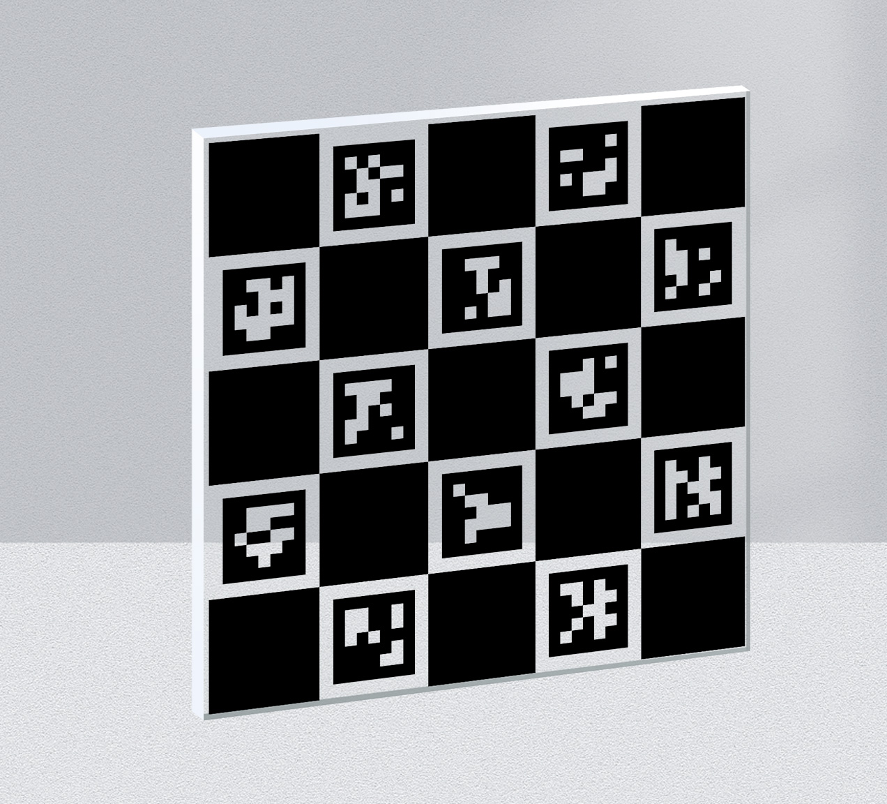
Charuco Calibration Board
Description: The Charuco Calibration Board combines the advantages of checkerboard patterns and ArUco markers, offering highly accurate and robust camera calibration. The checkerboard corners provide sub-pixel detection accuracy, while the ArUco markers enable automatic identification and corner indexing, even when only part of the board is visible. This makes it ideal for robotics, AR/VR, drone navigation, and computer vision research, where reliable calibration under challenging conditions is essential.
Product Details
The Charuco Calibration Board combines the advantages of checkerboard patterns and ArUco markers, offering highly accurate and robust camera calibration. The checkerboard corners provide sub-pixel detection accuracy, while the ArUco markers enable automatic identification and corner indexing, even when only part of the board is visible. This makes it ideal for robotics, AR/VR, drone navigation, and computer vision research, where reliable calibration under challenging conditions is essential.
Product Features: Micron-level high precision, high contrast, non-reflective, clear and easy to identify, High precision (with a maximum accuracy of 1um),supports multi-format drawing customization
Applicable scenarios: Machine vision calibration (security, film and television, medical, camera, drone camera, photography studio, scientific research instruments, and other equipment)
Calibration services:
The substrate for the Charuco Calibration Board is optional, and different substrates (such as glass, ceramic, aluminum plate, etc.) can be customized according to different usage scenarios, environments, and accuracy requirements.
In addition, as a system-level calibration solution provider, DFOPTIX can provide professional calibration technical services according to customer needs, including calibration technical consulting service support, calibration scenario-based engineering construction and other calibration solution services.
The following are some commonly used substrate parameter information:
1. Glass substrate parameters:
Design | Substrate | ||
Manufacturing Process | Photolithography | Glass substrate | Quartz glass (fused silica)/soda glass |
Minimum line width | 1µm / 0.55µm | Transmittance rate(@550nm) | >95% |
Feature accuracy | ±1µm | Coefficient of thermal expansion (20-200°C) | <5.0×10⁻⁷/K |
Coating | Yellow chromium, bright chromium , blue chromium (low reflectivity) | Expansion ratio(20-200°C) | 0.00006% (0.6µm/°C of 1m) |
Reflectance | < 13.4% @550nm | Surface flatness | <0.55µm (length<50mm) |
< 1.8% @650nm | <2µm (length<100mm) | ||
< 2.67% @750nm | <5µm (length>100mm) | ||
Coating accuracy | 120nm (±0.20nm) | Surface roughness | <0.025µm |
Optical density OD | Yellow Chromium 3 (Blue 5) | Thickness | 1mm、1.6mm、2.3mm、3mm(±0.2mm)(500*500*4.8) |
White background | Minimum line width:10µm | Minimum/maximum size | Min: 2×2 mm |
White background thickness: 40 µ m (smooth white coating on the back) | Max: 800×960mm (±0.1mm) | ||
Positive & negative shapes | Positive: pattern opaque Negative: pattern translucent | Appearance and shape | Square |
2. Ceramic substrate parameters:
Design | Substrate | |||||
Manufacturing Process | Photolithography | Type | Matte chromium on matte ceramics | Bright chrome on glossy ceramics | ||
Type | Matte ceramic | Glossy ceramic | Ceramic substrate | Zirconia / Alumina | ||
Minimum line width | 4µm | 2µm | Thickness | 1mm (±0.1mm, common) | 2mm (common) | 3mm (±0.1mm) |
Feature accuracy | ±2µm | ±2µm | Surface flatness | <30µm (length<100mm) | <60µm (length<200mm) | |
Appearance accuracy | ±0.05mm | ±0.05mm | Surface flatness | MIN: 2×2mm (±0.1mm); MAX: 228×228mm (±0.1mm) | ||
Coating | Chromium | Chromium | Surface roughness | <0.2-0.7µm | ||
Light coating/matte coating | Matte chromium coating | Bright chrome coating | Coefficient of thermal expansion (40-400°C) | <6.7×10⁻⁶/K | ||
ReflectaCnce | < 12.88% @550nm | < 9.56% @550nm | Unit weight | ≥ 3.66 g/cm³ | ||
< 10.62% @650nm | < 1.89% @650nm | |||||
< 12.23% @750nm | < 11.168% @750nm | |||||
Coating thickness | 100-120nm | 100-120nm | Rockwell hardness | ≥80 HRA | ||
Positive and negative shapes | Positive film: opaque pattern, Negative film: transparent pattern | Appearance and shape | Laser cutting of any shape | Square | Ellipse | |
Protective layer | The thin film above the chromium layer makes the chromium pattern more durable | Special shape | Punch | Chamfer | Oblique angle | |
3. Film substrate parameters:
Design | Film substrate | ||
Manufacturing Process | Lithography (Film Lithography Machine) | Application | Used for transmission/backlight /functional testing |
Minimum line width | 10 µ m/30 µ m optional | Coefficient of expansion | Film shrinks when heated and expands when cooled |
Feature accuracy
| ±10µm | 10µm/°C of 1m,When the relative temperature is constant, When the humidity changes by 1 ° C, A film with a length of 1m will change by 10 µ m (one ten thousandth) | |
Coating | Silver bromide | Transmittance rate(400~700nm) | >90% ultraviolet<(400~700nm)>infrared |
Coating thickness | 2µm | Film substrate thickness | 0.18mm (±0.01mm) |
Optical density OD |
OD>4 when 100% black (OD value controllable in grayscale)
| Maximum size | 0.71×0.81m (±0.1mm)(minimum line width 10µm) 1.68×3.5m (±0.1mm)(minimum line width 30µm) |
color | Black grayscale, sine grayscale | Appearance | Laser cutting, straight edge cutting, and circular hole hollowing are available |